-43_web.jpg)
Gibson Engineering & Computers, Inc. with 30+ years of manufacturing superior quality products is now making them available for your applications. Engineered and handcrafted in the United States for highest quality products at an affordable price.
With the volume of printed circuit boards (PCB), being produced in today’s market place, prices and lead-times have come down dramatically. Multi-layer PCBs are not restricted to the wealthy multi-national companies. Many times we find it is cheaper to go from schematics and simulations straight to a proto-type PCB due the low cost barriers.
The PCB process includes schematic creation, schematic capture, mechanical/physical parameters for the final assembly, component evaluation/selection, observing special conditions for signal paths/power/grounds/voltages/currents/thermal requirements, the PCB manufacturing process requirements and the PCB materials used. We strive to get you the right information to help you make informed decisions in the PCB process.
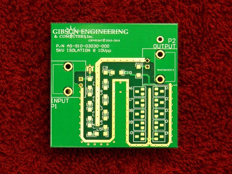
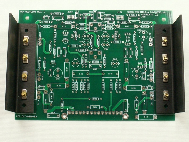
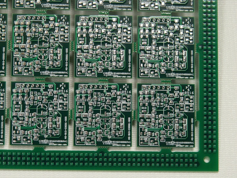
The sample photo is of a 4-layer two side loaded test design to demonstrate that we can manufacture a PCB locally at very near to the cost of overseas manufacturers without the risk of intellectual property lose. Due to the nature of PCB art and that intellectual property, it is hard to illustrate our capabilities. All sample PCAs on this site are the property of Gibson Engineering & Computers, Inc. Let us design a circuit board for your next project.